
Share
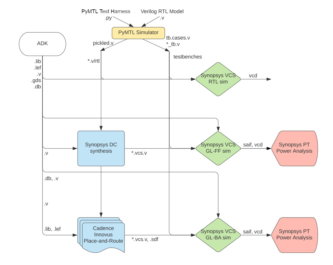
ECE 5745 Tutorial 4: Synopsys/Cadence ASIC Tools
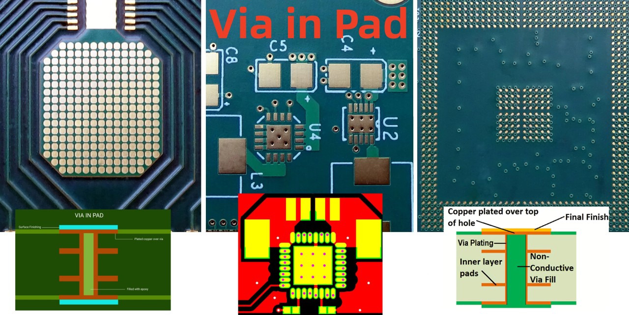
Via in Pad PCB Design
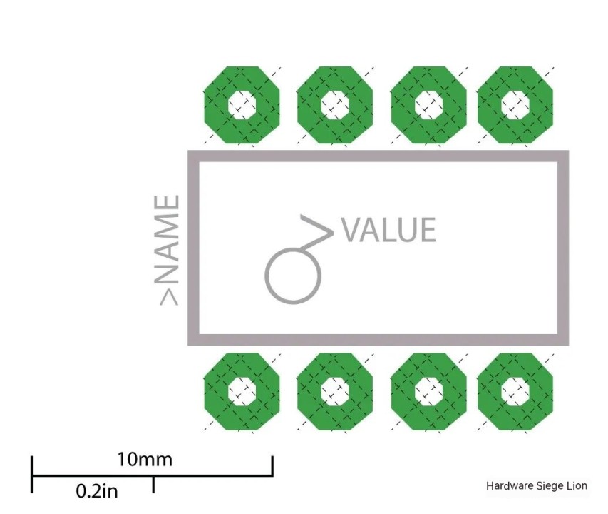
PCB pad design principles

Test board layout of a single layer FR4 board (5 cm 2 7 cm) with daisy
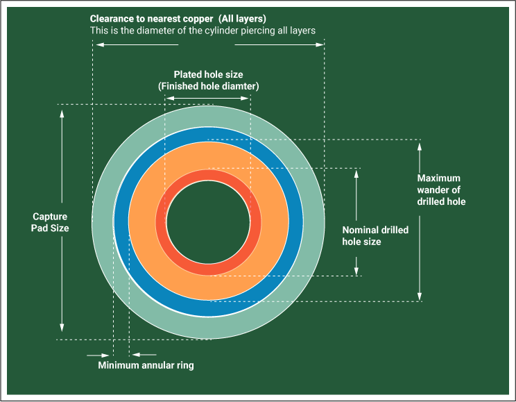
What is a Pad in PCB Design and Development

David WHALLEY, Visiting Fellow, B.Sc. M.Phil.

How to Design a BGA? - RAYPCB
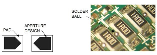
5 Key Design Features of an Effective Solder Paste Stencil

PCB Design Considerations and Guidelines for 0.4mm and 0.5mm WLPs

Details of test chip designs: pad pitch, layout, materials, and
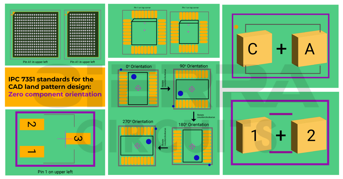
IPC 7351 Standards to Design a Footprint
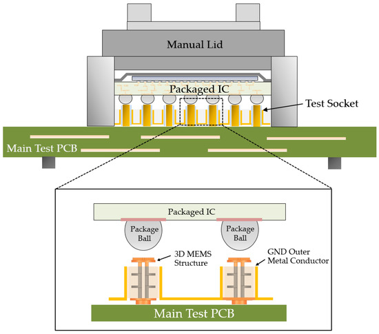
Sensors, Free Full-Text

PCB Stack-Up: Plan, Design, and Manufacture

Advanced Packaging Part 1 – Pad Limited Designs, Breakdown Of Economic Semiconductor Scaling, Heterogeneous Compute, and Chiplets
Related products
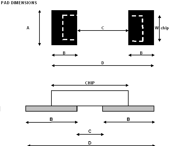
Pad Layout - Johanson Technology
Asking ipad pro 11 (2018) experts about chips on motherboard (see picture). : r/iPadPro
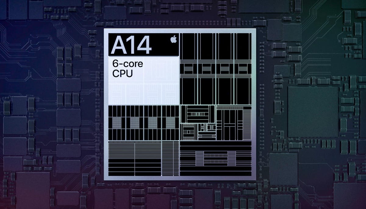
Apple boosts iPad Air performance 40% with new A14 Bionic chip - CNET

JC Romeo2 Dot Projector Chip JCID Face ID Integrated IC Dot Matrix Lattice IC For iPhone X-15ProMax Pad Pro 3/4/5 Face ID Repair
You may also like
160pcs/lot Band Aid Transparent Waterproof Breathable Adhesive Bandage First Aid Emergency Kit First Aid Bandaid - AliExpress

ITALIAN DESIGNER MAROON UNDERWIRE BRA - (32A/32B/30B)

Fleur D'Éclipse novo Floratta Eau de Parfum do Boticário - Natimus

High Waist Womens Shorts for Summer Loose Denim High Waisted Shorts Women Denim Solid Tummy Control Western Casual, Dark Blue, X-Small : : Clothing, Shoes & Accessories